
 English
 français
 Deutsch
 русский
 italiano
 español
 Nederlands
 العربية
 български
 svenska
2026-07-15
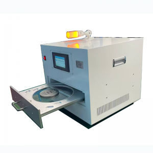
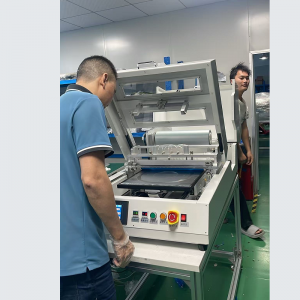
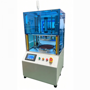
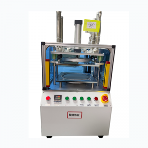
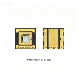
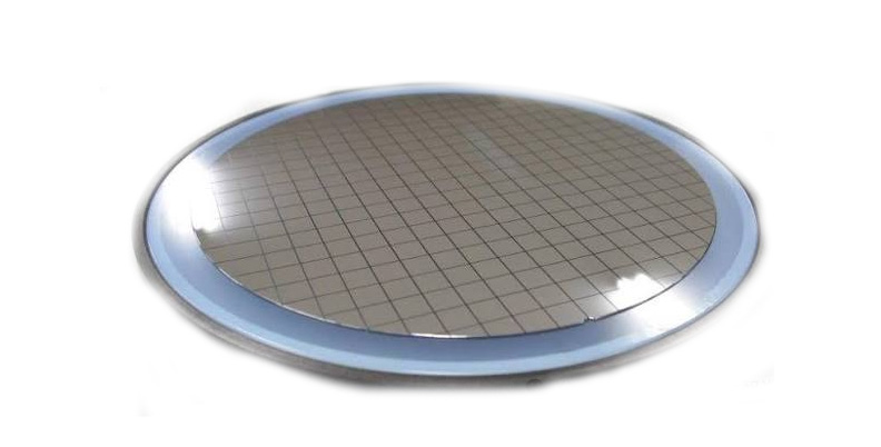
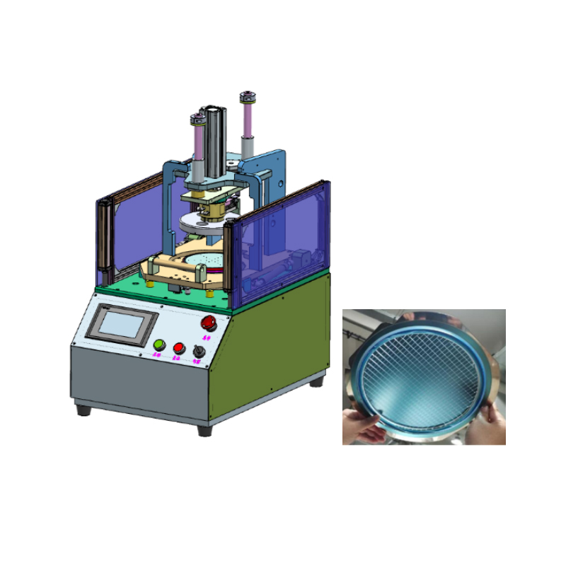
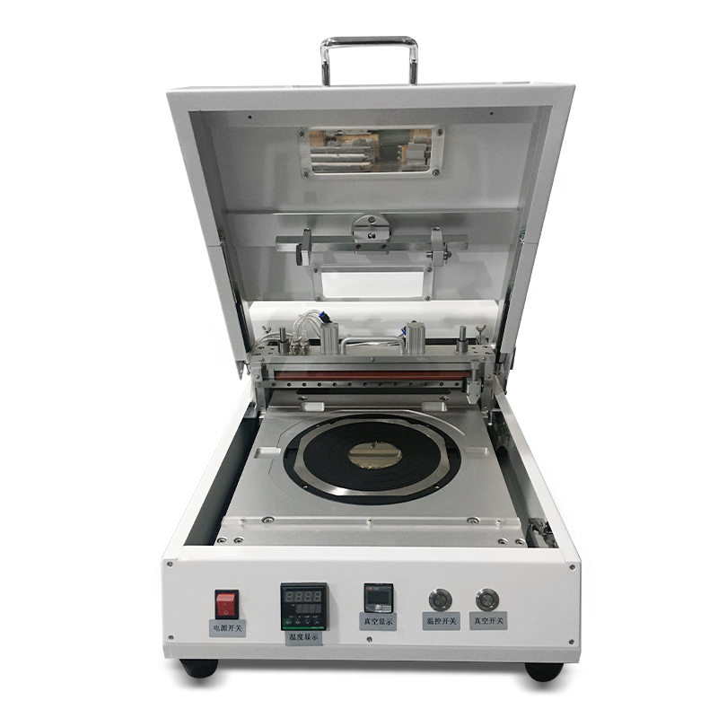
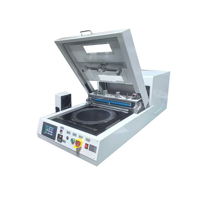
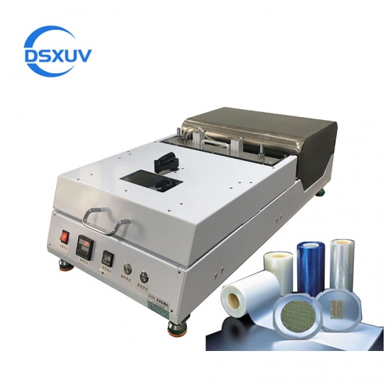
In the backside thinning process of a wafer, the thin film attached to the front side of the wafer (including the active device and microstructure side) is called a backside thinning tape (BG Tape or thin film in the industry) Its core function is to protect the integrated circuits and micro bumps on the front side of the wafer from physical scratches, contamination by grinding fluid and silicon p...
continue reading


 +8618924372460
 live:1651063690jennifer
 uvcure@uvspacelight.com
 0086-18924372460