2025-11-04 16:33:01
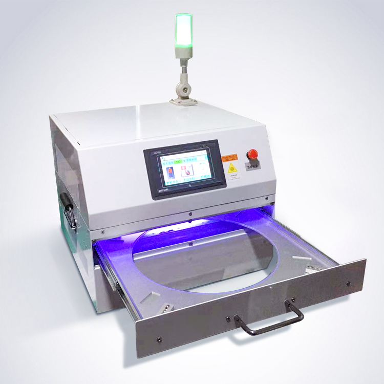
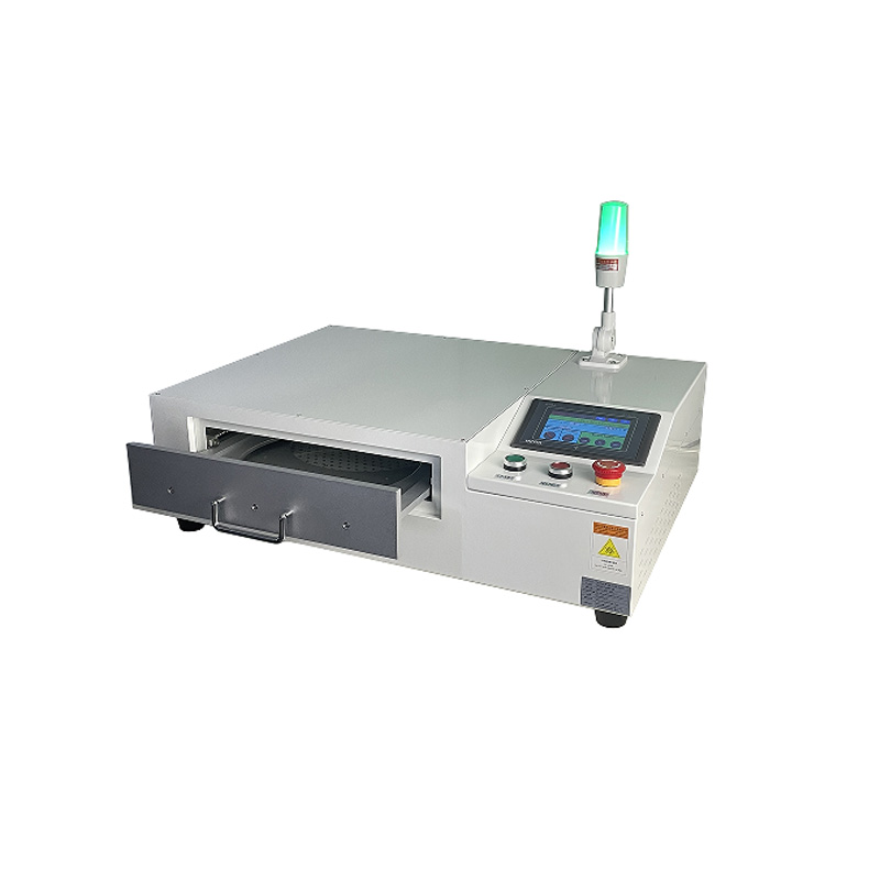
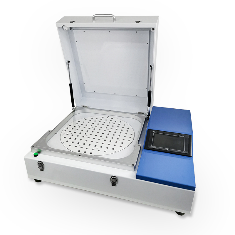
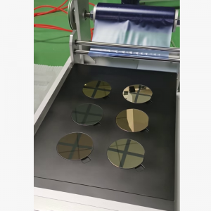
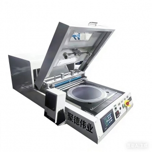
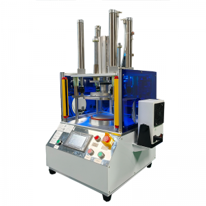
The wafer uv curing system machine is a key equipment used in semiconductor manufacturing to remove fixed adhesives. It uses UVLED ultraviolet light irradiation to reduce or decompose the viscosity of the adhesive, and is mainly used in the packaging process after chip slicing to improve production efficiency and product quality.
The wafer uv curing system plays a bridging role in the semiconductor packaging process
After slicing, debonding: Before chip slicing, the wafer frame needs to be fixed with a slicing adhesive film. After slicing is completed, the adhesive film is cured and hardened by UV light irradiation, reducing the adhesion of the fixing film and facilitating the peeling of the wafer or chip in subsequent packaging processes.
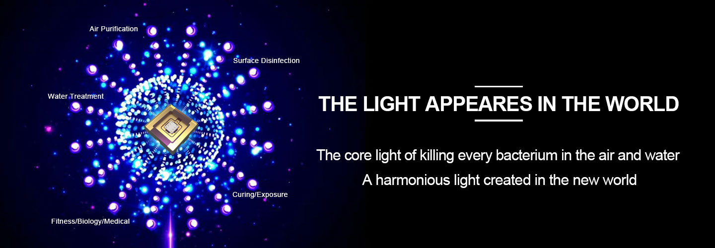
Wide applicability: In addition to semiconductor packaging, it is also used for UV debonding processes of materials such as glass cutting, ceramic processing, optical lenses, and LED integrated chips
Working principle and advantages:
working principle
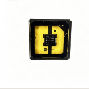
The ultraviolet light (wavelength 365nm-405nm) generated by UVLED irradiates the glue, causing photochemical reactions in the molecules to achieve curing, decomposition, or degradation.
Core strengths
1. Cold light source has no thermal radiation, avoiding thermal damage to the wafer
2. Long lifespan (about 20000 hours), far exceeding traditional mercury lamps
3. High photoelectric conversion efficiency, saving more than 30% energy
4. Closed design to prevent UV leakage, high safety
Improve production efficiency: Automated debonding process reduces manual intervention, combined with intelligent temperature control and programmable parameters, to adapt to different specifications such as 6inch 8 inch 12 inch wafers
Environmental Protection and Cost Optimization: No need for chemical solvents, reducing environmental pollution; Low energy consumption and long-life design reduce long-term operating costs
Guangdong Spacelight Technology Co., Ltd.
Tel :
0086-18924372460Fax :
0086-0755-27289230Email :
uvcure@uvspacelight.comSkype :
live:1651063690jenniferWhatsapp :
+8618924372460


Copyright Guangdong Spacelight Technology Co., Ltd.

 English
 français
 Deutsch
 русский
 italiano
 español
 Nederlands
 العربية
 български
 svenska
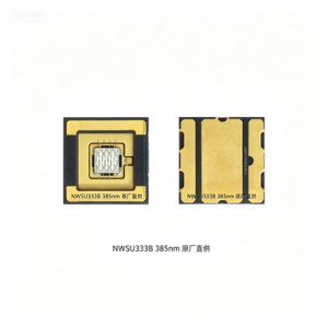
 +8618924372460
 live:1651063690jennifer
 uvcure@uvspacelight.com
 0086-18924372460