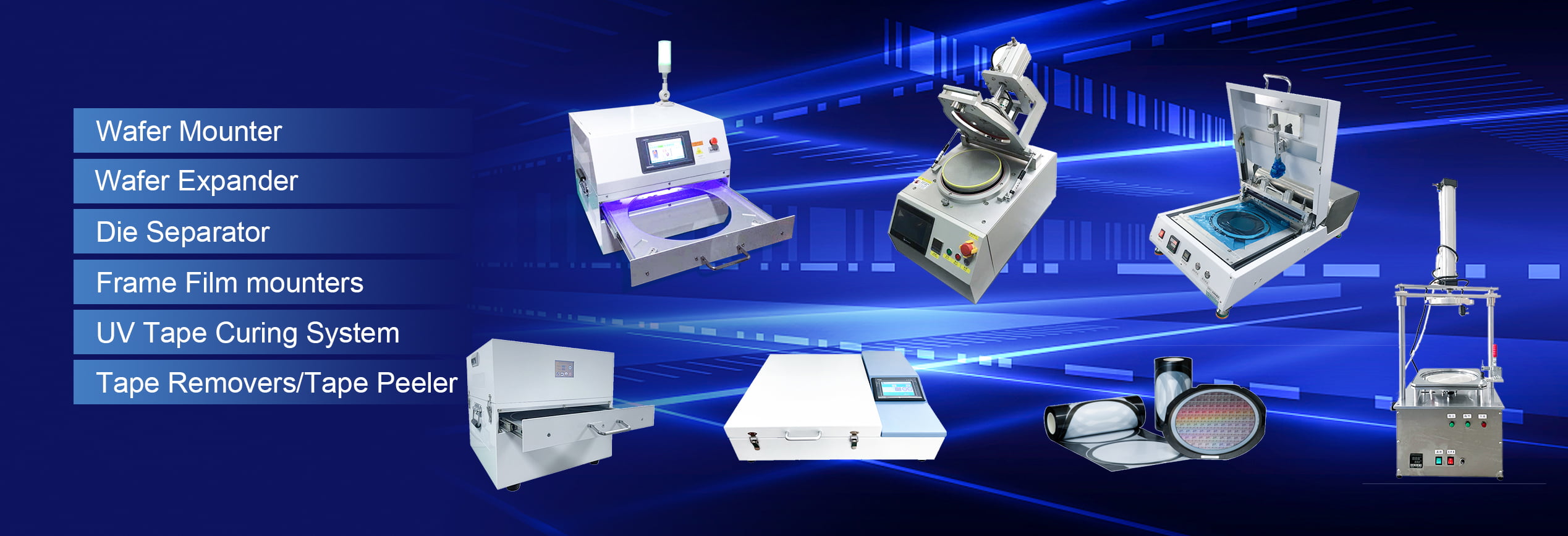
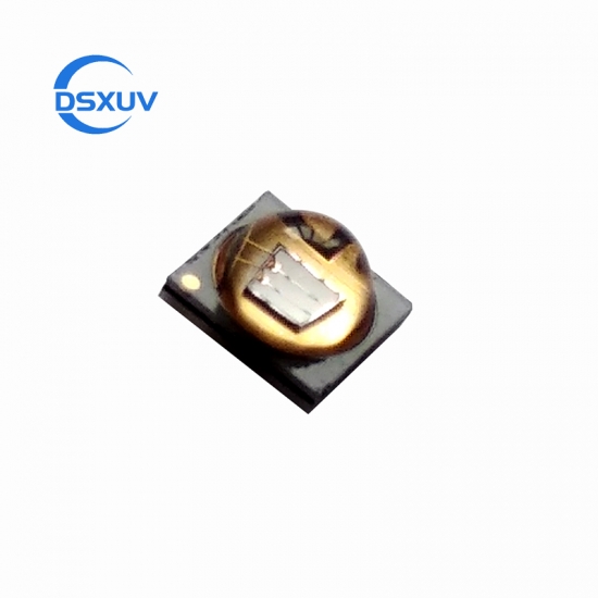
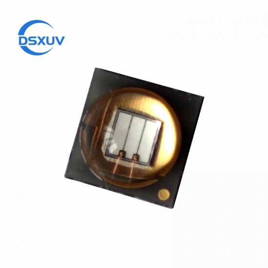
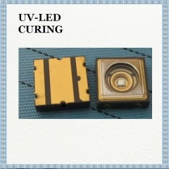
Key applications of SVC CUN66A1B 3W UV LED 3535 365nm are UV Curing, printing, coating, adhesive, counterfeit, detection/secuirty, UV torch, fluorescence,photography, dental curing, crime inspection, oil leak detaction, insect trap.
model no. :
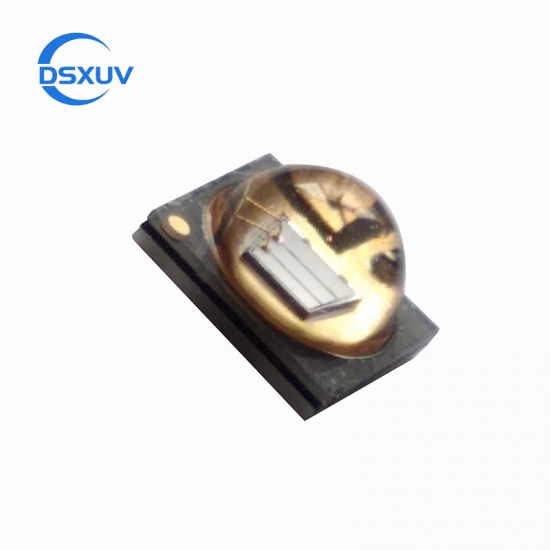
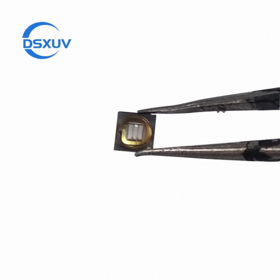
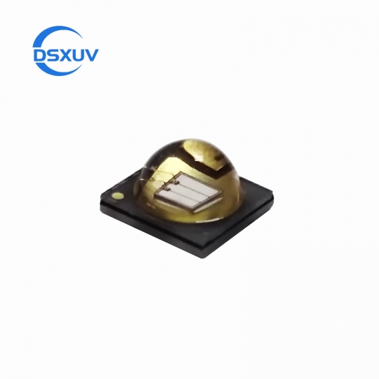
CUN66A1B UV LEDBrand:
DSXUVport of dispatch :
SHENZHENPayment :
T/T 100% before shipmentoriginal region :
CHINA
SVC CUN66A1B 3W UV LED 3535 365nm series are designed for high current operation and high power output applications.It incorporates state of the art SMD design and low thermal resistant material.SVC CUN66A1B 3W UV LED 3535 365nm is ideal UV light source for curing, printing, and detecting applications.
Product Parameters:
Brand: Korea SVC
Type:CUN66A1B
Size:3.5*3.5mm
Wavelength:360-370nm
Radiant Flux:1000-1300mW
Forward Current/Forward Voltage:1400mA/3.0-4.4V
View Angle:55deg.
Lens:Silicon
Performance Characteristics

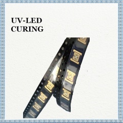
The PCB is made of aluminum and the size of PCB is 2.5cm by 2.5cm
Mechanical Dimensions

Reliability Test

Handling of Silicone Resin for LEDs

Precaution for Use
Pay attention to the following:
(3) Do not apply mechanical force or excess vibration during the cooling process to normal
 High Power UV-LED NVSU333A U365nm 18.9W 3640mW/cm2
NVSU333A UV-LED is widely used in high precision curing, ink curing (printing), bill checker etc. It's also the best way to solidify UV glue.
 NICHIA UV LED NVSU233B U365nm
NICHIA UV LED NVSU233B U365nm is most applied in UV curing, splicing, UV glue, and UV prinying ink curing.
 NICHIA NCSU033B 365nm UV LED
NICHIA NCSU033B 365nm UV LED can be used for criminal investigation, such as the observation of fingerprint, bloodstain, etc., mineral fluorescence observation, oil cleaning observation, and so on.
 NICHIA UV LED NCSU033C U365nm
NICHIA UV LED NCSU033C U365nm is Pb-free reflow Soldering application, built-in EDS protection Device, RoHS compliant.
 SVC CUN6GF1A UV 365nm 5W High Radiant Flux 1300mW
The applications of SVC CUN6GF1A UV 365nm 5W High Radiant Flux 1300mW are UV curing, printing, coating, adhesive, counterfeit dection/security, UV torch, fluorescence, photegraphy, dental curing, crime inspection, oil leak detection.
 High Power NICHIA UV LED NCSU276A U365nm for UV Curing
NICHIA UV LED NCSU276A U365nm requires unique and delicate production process. NICHIA places strict controls from wafer manufacturing to final inspection.
Guangdong Spacelight Technology Co., Ltd.
Tel :
0086-18924372460Fax :
0086-0755-27289230Email :
uvcure@uvspacelight.comSkype :
live:1651063690jenniferWhatsapp :
+8618924372460


Copyright Guangdong Spacelight Technology Co., Ltd.

 English
 français
 Deutsch
 русский
 italiano
 español
 Nederlands
 العربية
 български
 svenska

 +8618924372460
 live:1651063690jennifer
 uvcure@uvspacelight.com
 0086-18924372460