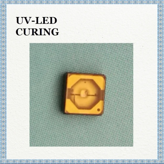
Key applications of UVB310nm CUD1GF1A LED are disinfection, fluorescent, spectroscopy, chemical and biological analysis. Also, it can be used in medical treatment for treat vitiligo.
model no. :
LED CUD1GF1A UV B310nmBrand:
DSXUVport of dispatch :
SHENZHENPayment :
T/Toriginal region :
CHINALead Time :
The Same DayFeatures anf Benefits of UVB310nm CUD1GF1A LED are deep ultraviolet LED, low thermal resistance, SMT solderable, lead free product, RoHS complicant.
Key applications of UVB310nm CUD1GF1A LED are disinfection, fluorescent spectroscopy, chemical and biological analysis.
Performance Characteristics

Notes :
1. Peak Wavelength Measurement tolerance : ±3nm
2. Radiant Flux Measurement tolerance : ± 10%
3. Φ e is the Total Radiant Flux as measured with an integrated sphere.
4. Forward Voltage Measurement tolerance : ±3%
5. Rθ J-S is the thermal resistance between chip junction to solder.
Mechanical Dimensions

Reliability Test

Handling of Silicone Resin for LEDs

Precaution for Use
(1) Storage
To avoid the moisture penetration, we recommend storing LEDs in a dry box with a desiccant . The
recommended storage temperature range is 5℃ to 30℃ and a maximum humidity of RH50%.
(2) Use Precaution after Opening the Packaging
Use proper SMD techniques when the LED is to be soldered dipped as separation of the lens may
affect the light output efficiency.
Pay attention to the following:
(3) Do not apply mechanical force or excess vibration during the cooling process to normal
(4) Do not rapidly cool device after soldering.
(5) Components should not be mounted on warped (non coplanar) portion of PCB.
(6) Radioactive exposure is not considered for the products listed here in.
(7) This device should not be used in any type of fluid such as water, oil, organic solvent and etc.
When washing is required, IPA (Isopropyl Alcohol) should be used.
(8) When the LEDs are in operation the maximum current should be decided after measuring the
package temperature.
(9) LEDs must be stored in a clean environment. We recommend LEDs store in nitrogen-filled
container.
(10) The appearance and specifications of the product may be modified for improvement without
notice.
(11) VOCs (Volatile organic compounds) emitted from materials used in the construction of fixtures ca
n penetrate silicone encapsulants of LEDs and discolor when exposed to heat and photonic energy. T
he result can be a significant loss of light output from the fixture. Knowledge of the properties of the m
aterials selected to be used in the construction of fixtures can help prevent these issues.
(12) The slug is electrically isolated.
(13) Attaching LEDs, do not use adhesives that outgas organic vapor.
(14) The driving circuit must be designed to allow forward voltage only when it is ON or OFF. If the rev
erse voltage is applied to LED, migration can be generated resulting in LED damage.
(15) LEDs are sensitive to Electro-Static Discharge (ESD) and Electrical Over Stress (EOS). Below is
a list of suggestions that Seoul Viosys purposes to minimize these effects.
a. ESD (Electro Static Discharge)
Electrostatic discharge (ESD) is the defined as the release of static electricity when two objects come
into contact. While most ESD events are considered harmless, it can be an expensive problem in
many industrial environments during production and storage. The damage from ESD to an LEDs may
cause the product to demonstrate unusual characteristics such as:
- Increase in reverse leakage current lowered turn-on voltage
- Abnormal emissions from the LED at low current
The following recommendations are suggested to help minimize the potential for an ESD event.
One or more recommended work area suggestions:
- Ionizing fan setup
- ESD table/shelf mat made of conductive materials
- ESD safe storage containers
One or more personnel suggestion options:
- Antistatic wrist-strap
- Antistatic material shoes
- Antistatic clothes
Environmental controls:
- Humidity control (ESD gets worse in a dry environment)
b. EOS (Electrical Over Stress)
Electrical Over-Stress (EOS) is defined as damage that may occur when an electronic device is
subjected to a current or voltage that is beyond the maximum specification limits of the device.
The effects from an EOS event can be noticed through product performance like:
- Changes to the performance of the LED package
(If the damage is around the bond pad area and since the package is completely encapsulated
the package may turn on but flicker show severe performance degradation.)
- Changes to the light output of the luminaire from component failure
- Components on the board not operating at determined drive power
Failure of performance from entire fixture due to changes in circuit voltage and current across total
circuit causing trickle down failures. It is impossible to predict the failure mode of every LED exposed
to electrical overstress as the failure modes have been investigated to vary, but there are some
common signs that will indicate an EOS event has occurred:
- Damaged may be noticed to the bond wires (appearing similar to a blown fuse)
- Damage to the bond pads located on the emission surface of the LED package
(shadowing can be noticed around the bond pads while viewing through a microscope)
- Anomalies noticed in the encapsulation and phosphor around the bond wires.
- This damage usually appears due to the thermal stress produced during the EOS event.
c. To help minimize the damage from an EOS event Seoul Viosys recommends utilizing:
- A surge protection circuit
- An appropriately rated over voltage protection device
- A current limiting device

 NICHIA UV LED NVSU233B U365nm
NICHIA UV LED NVSU233B U365nm is most applied in UV curing, splicing, UV glue, and UV prinying ink curing.
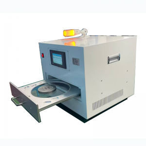
 Chip Film Transfer Molding Machine
Chip inversion machine can be used to transfer wafers from one film to another (such as UV film, blue film, optical film, etc.). This can be used to manufacture devices with specific functions, such as optical devices, sensors, and microelectronic components
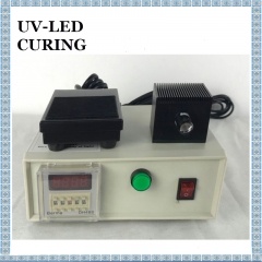
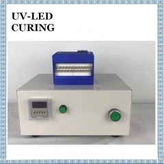
 104*25mm Water Cooling UV LED Curing System
The WnnexCureTM EB168 UV Light Emitting Diode provides highest output power in an extremely medium mechanical package for high speed pinning and full cure applications. The EB168 UV LED Light Source is CE, RoHS, and REACH compliant.
 365nm NVSU333A Highest Power UV LED Spot Light Source
NVSU333A 365nm UV LED Spot Light Source, highest Power UV 365nm LED Curing Lamp, instantly cure UV glue
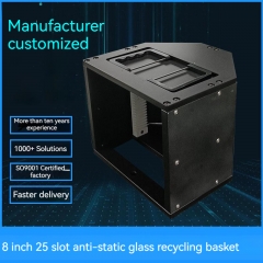 8 Inch 25 Slot Tank Glass Recycling Wafer Carrier
8 Inch 25 Slot Tank Glass Recycling Wafer Carrier 6061 Aluminum Antistatic High Precision Sandblasting Wafer Cassette High precision and flatness Advanced precision equipment processing, processing accuracy up to ±0.01mm, assembly flatness ±0.2mm, in line with the mainstream welding line, solid equipment technical requirements. Product Parameters Product Name: 8-inch 25-slot anti-static glass recycling basket Product code:DSXUV-20D08-000-R5 Product size: 241L)*224(W)* 200(H)MM Slot Number: 25 slots Slot Distance: 3mm Starting slot: 20mm Product process: precision machining/hard oxidation Quality: 6061 aluminum
 100*20mm 365nm UV LED Curing Systems for UV Glue Curing
100*20mm 365nm UV LED Curing Systems is instant drying, can inprove the suaface hearness of the coating and make the color bright. Fast curing speed, high production efficiency.
Guangdong Spacelight Technology Co., Ltd.
Tel :
0086-18924372460Fax :
0086-0755-27289230Email :
uvcure@uvspacelight.comSkype :
live:1651063690jenniferWhatsapp :
+8618924372460


Copyright Guangdong Spacelight Technology Co., Ltd.

 English
 français
 Deutsch
 русский
 italiano
 español
 Nederlands
 العربية
 български
 svenska
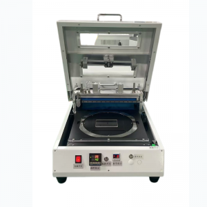
 +8618924372460
 live:1651063690jennifer
 uvcure@uvspacelight.com
 0086-18924372460