
2023-04-19 17:31:56
Are 0.25mm wafers thin or thick? How thin or how thick is suitable for a wafer? How is it divided?
A 0.25mm wafer can be considered a thin wafer, but it is not really a thin wafer. The thickness of wafers varies according to application requirements. Generally, wafers less than or equal to 100μm (0.1mm) can be considered thin, and wafers greater than 100μm can be considered thick. In engineering and scientific research fields, the classification criteria of thickness will be different due to the consideration of different application requirements.

Relative to the integrated circuit, a typical 4inch wafer is 0.52mm, 6inch wafer is about 0.67mm thick. The wafer needs to be thinned, otherwise it will take a lot of wear and tear on the blade, and it will cut two times. For DIP packaging, 4 "wafers should be thinned to 0.3mm and 6" wafers should be thinned to about 0.32mm, error 0.02mm. Measuring the thickness of the instrument piece with a micrometer will do. The film thickness is generally measured by thermal wave instrument. By measuring the thickness of different distribution points, the film thickness can be obtained by averaging, which generally reflects the uniformity of the film at the same time, and the simulation contour line can be seen. Germanium, silicon, selenium, gallium arsenide, and many metal oxides and metal sulfides, which are between conductors and insulators, are called semiconductors. Semiconductors have some special properties. The thermosensitive element (thermistor) for automatic control can be made by using the relation between the resistivity and temperature of the semiconductor. Using its photosensitive characteristics can be made into automatic control of photosensitive components, such as photoelectric cell, photocell and photoresistor. One of the most important properties of semiconductors is that their ability to conduct electricity is increased by millions of times if a small amount of impurities are properly added to a pure semiconductor material.

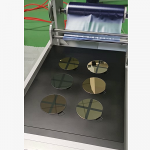
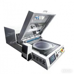
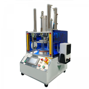
For wafer lamination machine / wafer mounter, wafer thickness is not the same, the selection of wafer laminating machine specifications are not the same. The mounting plate of wafer frame film mounter has a ceramic material plate, Teflon or other material mounting plate. Users must choose carefully according to their materials before purchasing.

Guangdong Spacelight Technology Co., Ltd.
Tel :
0086-18924372460Fax :
0086-0755-27289230Email :
uvcure@uvspacelight.comSkype :
live:1651063690jenniferWhatsapp :
+8618924372460


Copyright Guangdong Spacelight Technology Co., Ltd.

 English
 français
 Deutsch
 русский
 italiano
 español
 Nederlands
 العربية
 български
 svenska
 +8618924372460
 live:1651063690jennifer
 uvcure@uvspacelight.com
 0086-18924372460