2022-12-29 15:09:30
Bonding means attaching two objects together with a seal (often permanently)
Microtechnology involves various types of bonding processes
Used in IC packaging and printed circuit board assembly. Will not be covered in this lecture.
- Wafer bonding
- Wire bonding
- Flip chip bonding
Wafer bonding
1: as a way to make advanced starting wafers SOI)
2: as a way to create complex 3D structures and cavities which create device functionality(chambers,channels,nozzles...)
3: as a packaging method to create closed3environments(vacuum packages for resonators mirrors and IR devices)

Bonding requirements:
- smooth surfaces(on nm-scale)
- flat wafers (on cm-scale)
(intimate contact)
- no particles (voids larger than particles)
- matching CTEs (otherwise stresses)
- suitable surface chemistry (hydrophilic)
Wafer bonding procedure:
- particle removal
- surface chemistry modification
- (optional) vacuum pumping
- (optional) wafer alignment
- room temperature joining
- application of force/heat/voltage(optional) wafer thinning
Bonding considerations:
Bond properties
- What are the chemical bonds that will bond ?
- Exist naturally or formed by treatment?
- Bond strength ?
- Permanent vs. temporary ?
Bonding: materials
- Chemical compatibility
- Temperature tolerance
Bond formation temperature
Device operation temperature
- CTE(coefficient of thermal expansion) mismatch between materials
- Surface quality (roughness; waviness)
- Surface particles
Bonding: productivity considerations
- Availability of equipment (production tools have automated,cassette to cassette operation)
- Process compatibility (IC compatibility:temperature & contamination)
- Process yield
- Throughput
- Cost
- Maturity
Adhesive bonding
- surface cleaning
- spin coating of polymer
- initial curing (solvent bake)
- evacuate vacuum (optional)
- join the wafers
- final curing pressure and/or heat

Adhesive bonding benefits:
- temperatures around 100°C (>Tg)
- tolerant to (some) particle contamination
- structured wafers can be bonded
- low cost, simple process
Anodic bonding
- Anodic bonding (AB) = Field-assisted thermal bonding
- Glass and metals bonded
- Various glass types
Corning 7740 Pyrex glass most common for anodic bonding
CTE close to that of Si
- Annealing the glass before of after bonding can reduce stresses due to CTE mismatch

Fusion/direct/thermal bonding:
- Identical materials bonded
- No CTE problems
- Bonds naturally available
- Apply heat/pressure to enhance bonding
- Si-Si
- Glass-glass
- Polymer-polymer
Polymer thermal bonding (1):
Raise temperature above Tg
>softening
>intimate contact (hold long enough)>cool down below Tg
>Bond interface indistinguishable from bulk materials (because same bonds !)

Polymer bonding (2):
Softening by solvent surface treatment
>Intimate contact (hold long enough)
>Bonding of different polymers, too!
>In theory a room temperature process
>In practise difficult to control the thickness of the softened layer
C-SOl assignment
You are a SOl wafer manufacturer.
You would like to offer C-SOl wafers to your customers.
This brings about many technical issues as each design unique:
- SOl device layer thickness BOX-thickness
- cavity depths
- chip size
- film or no film at cavity bottom-what processes will be done afterwards ?
- ......
C-SOI commercial/contractua
You need to collaborate with the buyer more intimately:
- share designs
- share processing
- ship wafers around
- agree on inspections/quality
Develop a business model for C-SOI!
Output:
A PowerPoint presentation that you will present to potential MEMS manufacturers trying to presuade them to adopt C-SOl.
Audience includes engineers and bosses.
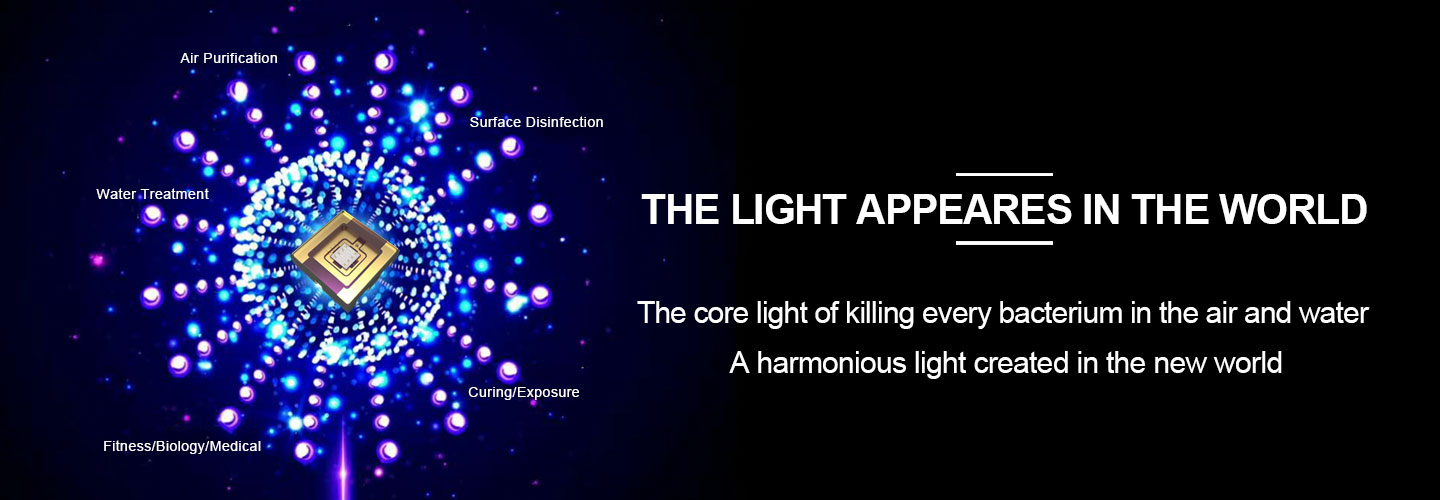
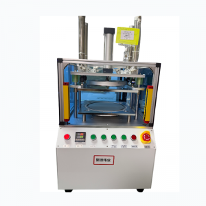
Guangdong Spacelight Technology Co., Ltd.
Tel :
0086-18924372460Fax :
0086-0755-27289230Email :
uvcure@uvspacelight.comSkype :
live:1651063690jenniferWhatsapp :
+8618924372460


Copyright Guangdong Spacelight Technology Co., Ltd.

 English
 français
 Deutsch
 русский
 italiano
 español
 Nederlands
 العربية
 български
 svenska
 +8618924372460
 live:1651063690jennifer
 uvcure@uvspacelight.com
 0086-18924372460