model no. :
DSX26-050Brand:
DSXUVport of dispatch :
SHENZHENPayment :
TT 100%original region :
SHENZHENLead Time :
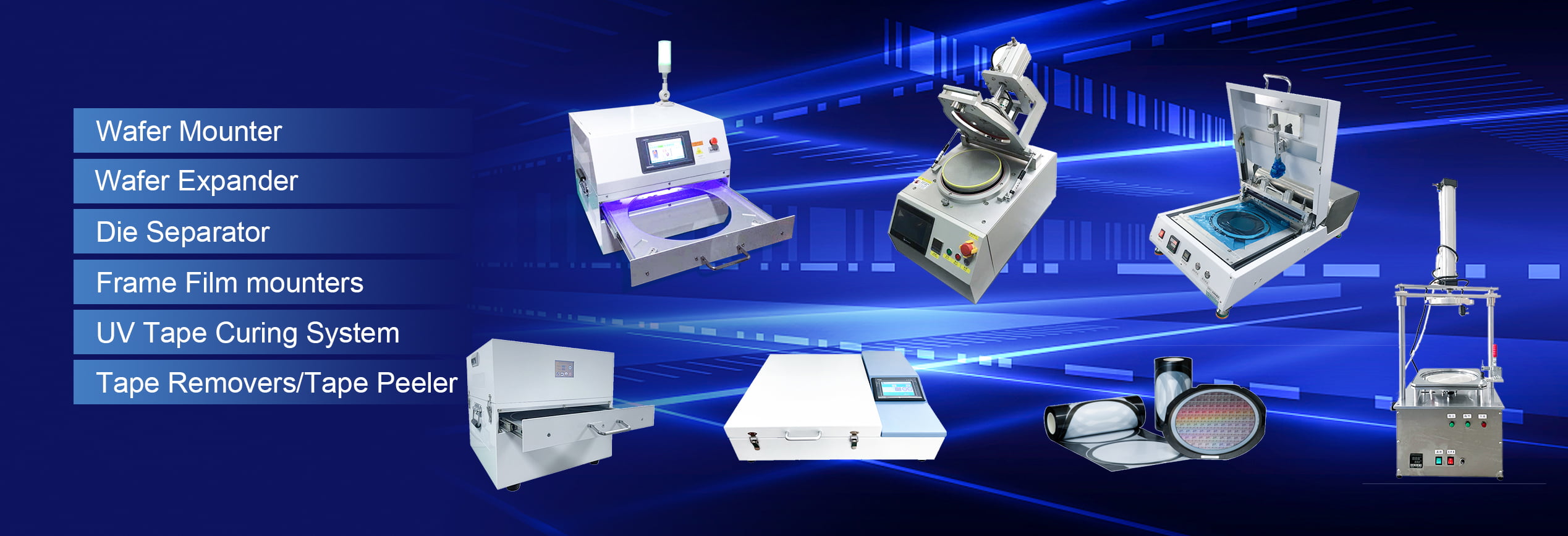
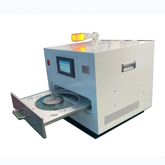
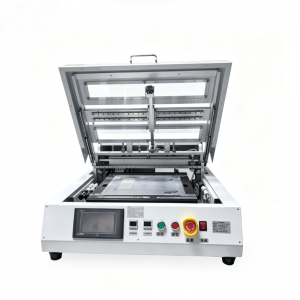
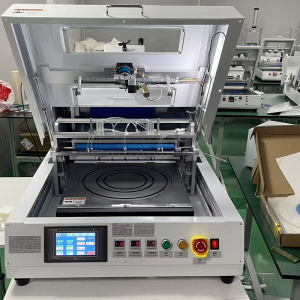
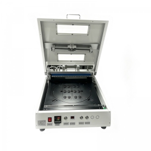
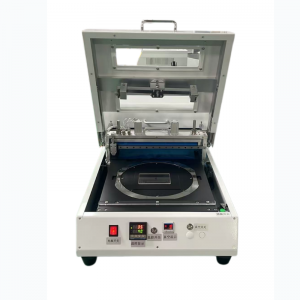
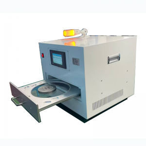
15DAYS10 Inch Wafer Frame with N2 Nitrogen UV Debonding Machine, Semiconductor Wafer UV Tape Degumming Equipment With Touch Screen & Alarm Function.
Product Parameters
|
Model |
DSXUV-N2-8 |
Manufacturer |
Dongguan Jude Weiye Electronic Technology Co., Ltd. |
|
Size |
L516*W510*H450mm |
Compatible Size |
Compatible with 10-inch iron rings |
|
Drawer Height |
30mm |
Curing area |
Φ250mm |
|
Wavelenth |
UVLED365nm |
Power |
1000W |
|
UV intensity |
400mW/cm2 |
Input |
100-240V AC 50-60HZ |
|
Material |
White sheet metal /55kg |
Cooling |
Air |
|
Irradiation direction |
From bottom to top |
Display/Language |
Touch screen/EN CN... |
|
1.Configuration & requirement
|
||||||||||||||||||||||||||||||||||||||||||||||||||||||||||||||||||||||||||||||||||||||||||||||||||||
|
2.1All process Specifications should be based on 6 inch Si &SiC wafer
Tool must be able to handle substrate with the following specifications,good Si & SIC 6inch wafer handling and process performance. 6inch silicon carbide wafer substrate specifications 6 inch
|
||||||||||||||||||||||||||||||||||||||||||||||||||||||||||||||||||||||||||||||||||||||||||||||||||||
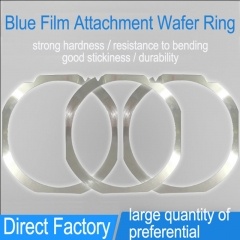 6 Inches Dicing Wafer Frame Iron Hoop Semiconductor Fixed Cutting Ring SUS420J Material
6 inches Wafer Expander Rings is used for semiconductor packaging, film, cutting, adhesive process bearing appliances.
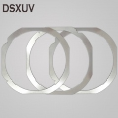 12 inches Wafer Frame Dicing Cutting Ring Round Fixed Silicon Disk Iron Ring For Wafer Blue Film
Stainless Steel 12'' Iron Ring Wafer Frame is strong hardness, resistance to bending, good stickiness, durability.
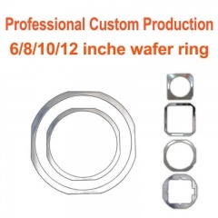 Customized 6 8 12 inch Crystal Iron Ring Wafer Cutting Film Hoop for Wafer Foundry
The selection material of Stainless Steel Wafer Iron Rings is through SGS certification, high bending strength, high hardness, can bear high load, high wear, corrosive media.
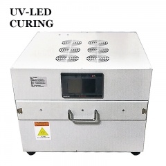 Nitrogen UV Curing Systems Multiple 6 inches Wafer Dicing Machine
Curing multiple 6 inches UV Wafer at the same time, UV Film Tape Curing Systems reduce the adhesive strength of all UV-sensitive dicing tapes under controlled environment.
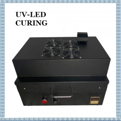 Customized UV LED Cold Light Source UV LED Exposure Unit 365nm 395nm
Professional Manufacturing UV Wafer Tape Curing Machine is low calorie, good bonding performance, fast speed, environmental protection equipment.
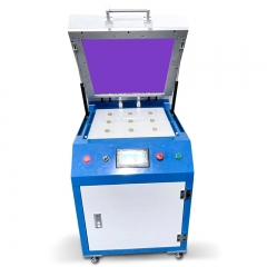 Clamshell 500*500mm UV Tape UV Curing Systems Reducing Blue Film Viscosity
Adhesive strength becomes lower when UV(Ultraviolet light) is irradiated by UV Tape UV Curing Systems.
Guangdong Spacelight Technology Co., Ltd.
Tel :
0086-18924372460Fax :
0086-0755-27289230Email :
uvcure@uvspacelight.comSkype :
live:1651063690jenniferWhatsapp :
+8618924372460




Copyright Guangdong Spacelight Technology Co., Ltd.

 English
 français
 Deutsch
 русский
 italiano
 español
 Nederlands
 العربية
 български
 svenska


 +8618924372460
 live:1651063690jennifer
 uvcure@uvspacelight.com
 0086-18924372460