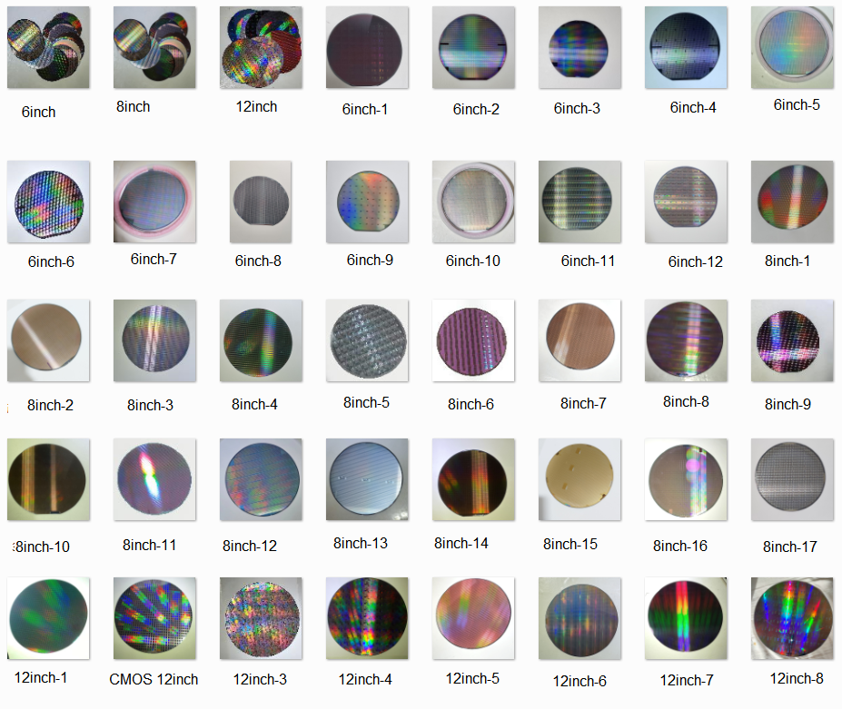
There are various specifications and types of wafers. Here are some common wafer specifications and types:
1. Diameter: The diameter of a wafer is one of the most commonly used specifications. Common diameters include:
- 200mm: also known as 8-inch wafers.
- 300mm: also known as 12-inch wafers.
- 150mm, 100mm, 75mm, 50mm, etc.
2. Thickness: The thickness of wafers is usually controlled and adjusted during the manufacturing process. Common thickness ranges include:
- 650μm: commonly used in earlier processes.
- 550μm, 450μm, 380μm: as technology advances and processes shrink, the thickness decreases.
- Ultra-thin wafers: In some advanced processes, wafer thickness can be much smaller than traditional thicknesses, reaching below 100μm.
3. Substrate Materials: Wafers can be made from various substrate materials. Common materials include:
- Silicon (Si): The most common substrate material used extensively in semiconductor manufacturing.
- Silicon Carbide (SiC): Used for high-power electronic devices and optoelectronic device manufacturing.
- Gallium Nitride (GaN): Used for LED and high-power electronic devices manufacturing.
- Sapphire (Al2O3): Used for optoelectronic device manufacturing.
4. Structure Types: Wafers can have different structural types. Some common classifications include:
- Silicon-on-Insulator (SOI): Wafers with a certain thickness of insulating layer, commonly used for high-performance integrated circuit manufacturing.
- Stacked wafers: Wafers stacked together for 3D packaging and integration.
- Composite wafers: Wafers that integrate different materials to meet specific application requirements.
These are just some of the common wafer specifications and types. In reality, there are many other specifications and types available to meet the requirements of different application fields.
Where can you buy such wafers?
DSXUV provides a wide range of wafer substrates. For technical consultation, please contact our customer service.




 English
 français
 Deutsch
 русский
 italiano
 español
 Nederlands
 العربية
 български
 svenska


 +8618924372460
 live:1651063690jennifer
 uvcure@uvspacelight.com
 0086-18924372460